Building the Simple 8085 Computer
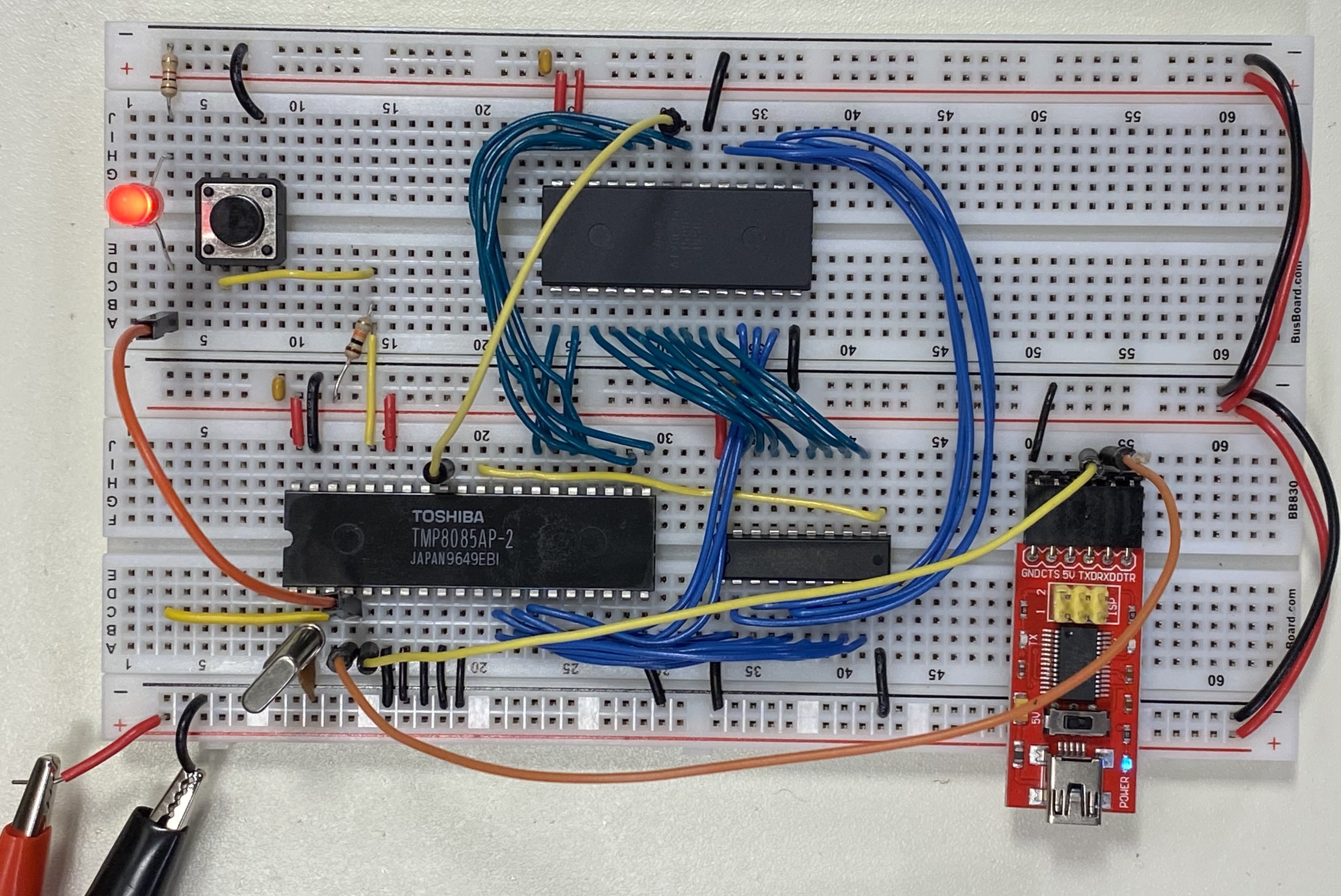
Initially, the system was prototyped on a solderless breadboard in the hopes that some basic functionality could be proven before spinning a real PCB. Starting with the 8085 chip, functionality was tested as new components were added.
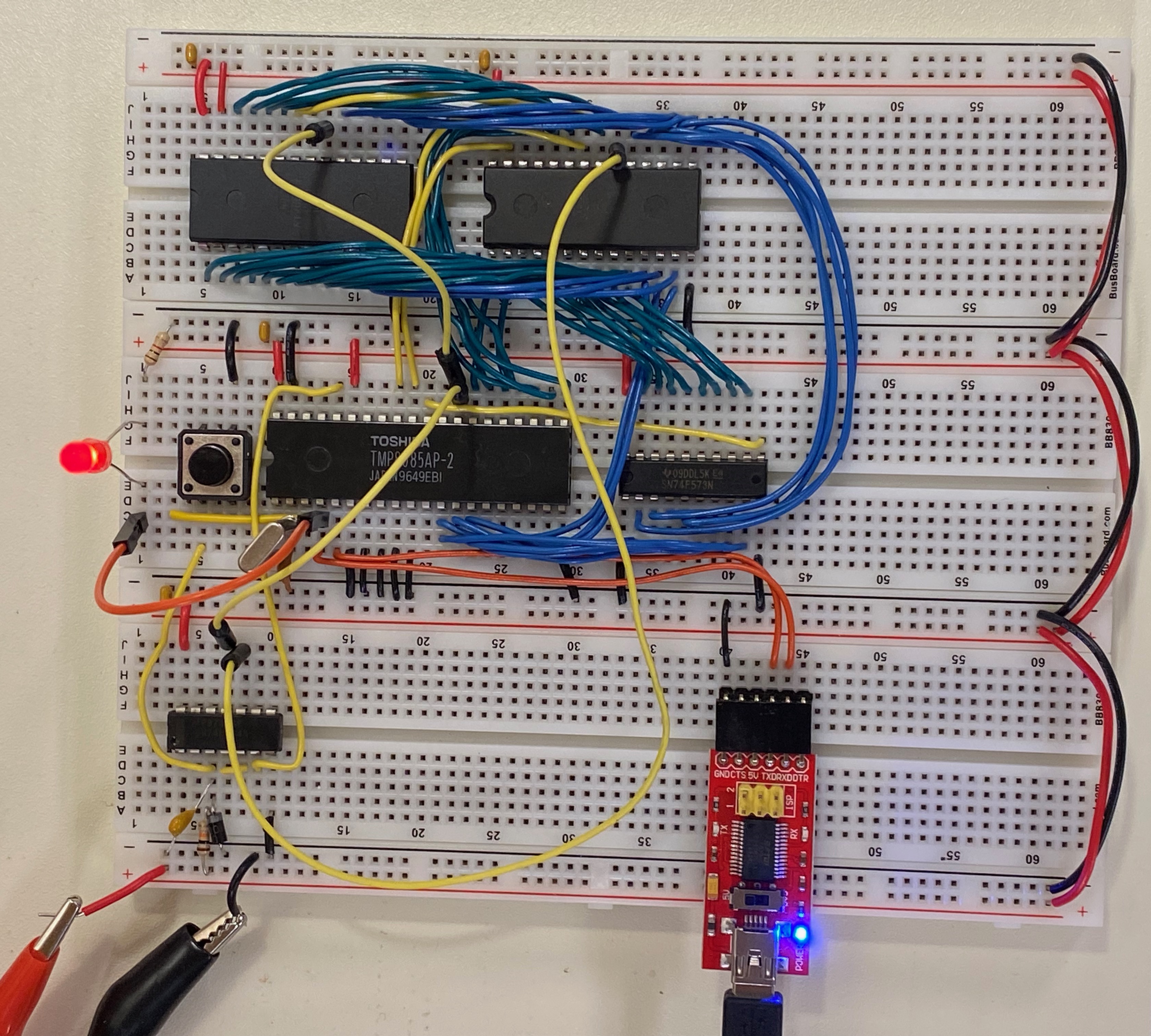
A new build was recently completed to document each step of the process. Schematics for each step were drawn in KiCad and are available in the repo.
Step 1: Free-run Test


The first test was to wire up the processor with pull-down resistors on the data lines, forcing it to read a NOP for every instruction read. This cycles though the entire address range forever and proves the basic processor functionality. If the test is working correctly, the A15..A8 address lines will all toggle, with A14 twice as fast as A15, A13 twice A14, and so on. This can be observed with an oscilloscope or logic analyzer, or even an LED and resistor on the top address lines if a slower clock crystal is used.
This test passed and produced a cool light show when LEDs were wired to the address lines.
The only parts needed for this are the 8085, clock crystal, and eight resistors for the AD0..AD7 lines.
- wire the X1 and _X2 to the crystal, as in the final schematic
- connect each ADn line to GND though a 1K or similar resistor
- connect SID, HOLD, INTR, TRAP, and the RSTn lines to GND
- connect READY and RESET_IN to 5V
- leave other signals unconnected, including RD, WR, SOD, and ALE
Step 2: ROM

The next test was to wire in the address/data latch and to connect the EEPROM. An initial test program was loaded that blinks an LED from the SOD line. The RESET button was also added at this point.
To add the ROM to the 8085, make the following connections as in the final schematic:
- 8-bit latch control and inputs to the ALE and AD0..7 lines
- EEPROM A0..A7 to the address latch outputs
- data pins of the EEPROM to AD0..7
- EEPROM A8..14 to the 8085 A8..14
- EEPROM OE to RD
- EEPROM WE to 5V
Also connect the following:
- 8085 SOD to an LED and resistor to GND
- EEPROM CE to GND (this maps the ROM base address at both 0000 and 8000)
- RESET_IN to +5V through a 10K resistor and also to GND through a pushbutton
Burn the ROM LED test program into the EEPROM at starting address 0000H. Note that this program starts with a JMP instruction to clear the reset flip-flop. This isn’t needed, but means that the program will also work if the final address decoding hardware is installed.
If the test above suceedes, basic ROM wiring has been verified. A second test program can now be run to verify that all of the upper ROM address lines have been connected correctly. It will flash the LED at different speeds for a successful test or do a continuous fast blink on failure.
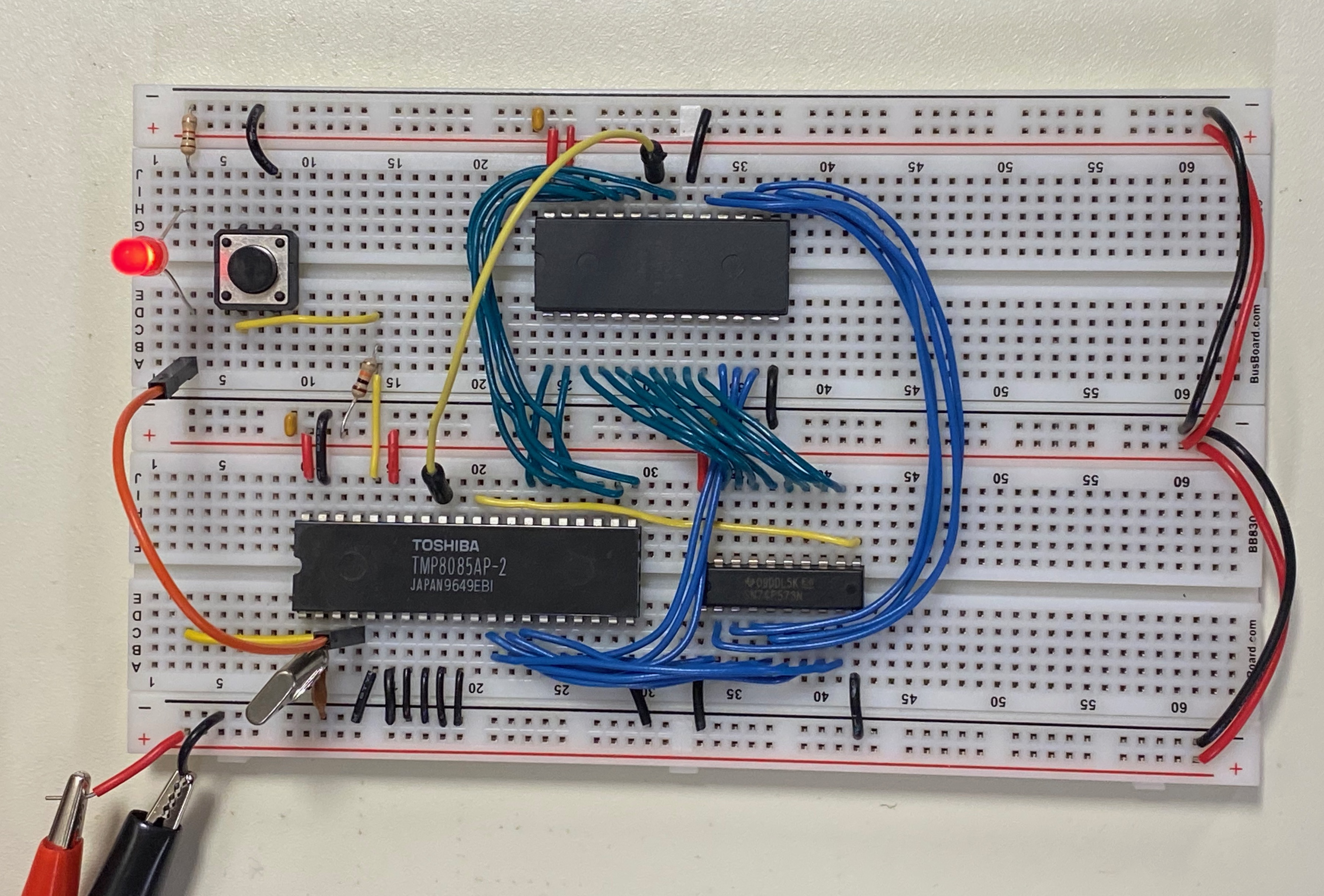
Step 3: Serial Communications

The next test, with the same basic hardware, was to wire in the FTDI chip to the SOD and bit-bang a character out as async serial data. The ROM serial test program writes a continuous stream of the ‘T’ character to the serial port.
- connect an FTDI interface to GND, SID and SOD as shown in the final schematic
Note that this program uses timing loops that are dependent on the frequency of the clock crystal. A different crystal would require different delay loop values. The connected termnal should be set for 9600bps.
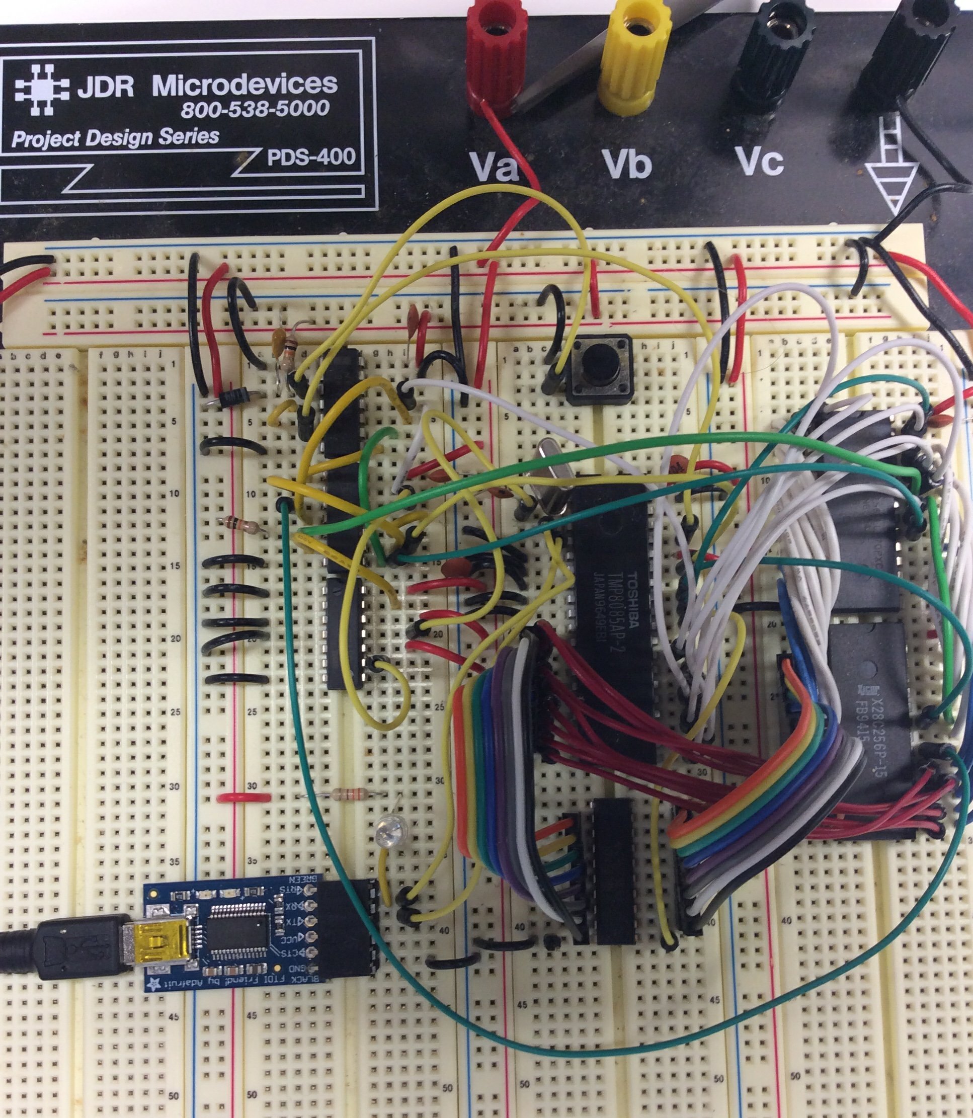
Step 4: RAM
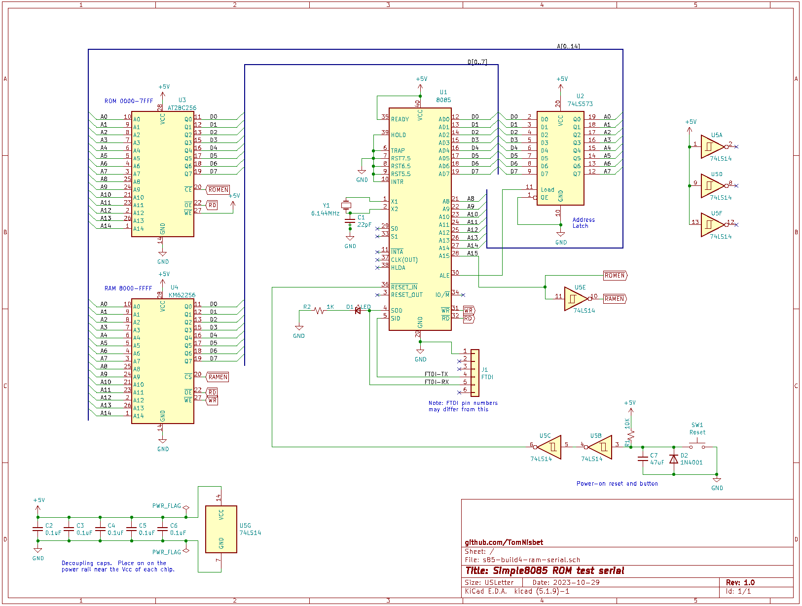
The next test was to wire in the RAM chip and modify the test program to write some characters to RAM and read them back before outputting them as serial data. The reset circuit was also expanded to include the power-on reset in addition to the existing button.
Note that the RAM was installed where the ROM was previously located and the ROM was moved to the left where there are fewer wires. This was done to make it easier to remove the ROM for programming. Other than the WE and CE pins, all other connections for the RAM and ROM are identical.
To add the RAM to the 8085, make the following connections as in the final schematic:
- RAM A0..A7 to the address latch outputs
- data pins of the RAM to AD0..7
- RAM A8..14 to the 8085 A8..14
- RAM OE to RD
- RAM WE to WR
Also connect the following:
- EEPROM CE to 8085 A15 (this maps the ROM base address at 0000)
- RAM CE to inverted 8085 A15 (this maps the RAM base address at 8000)
- complete the reset circuit with the addition of the inverters, capacitor, and diode
The RAM serial test program writes a continuous string of A to Z characters to the serial port.
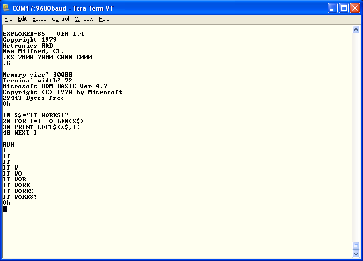
Now that RAM is working, code development can be sped up with the use of the Hex Loader. This can be burned into the ROM and will load and execute programs from RAM. While not as powerful as a full monitor, it does remove the need to power down the system and remove the ROM for each code update. It accepts Intel Hex files from asm85 or other tools that write in the standard format.
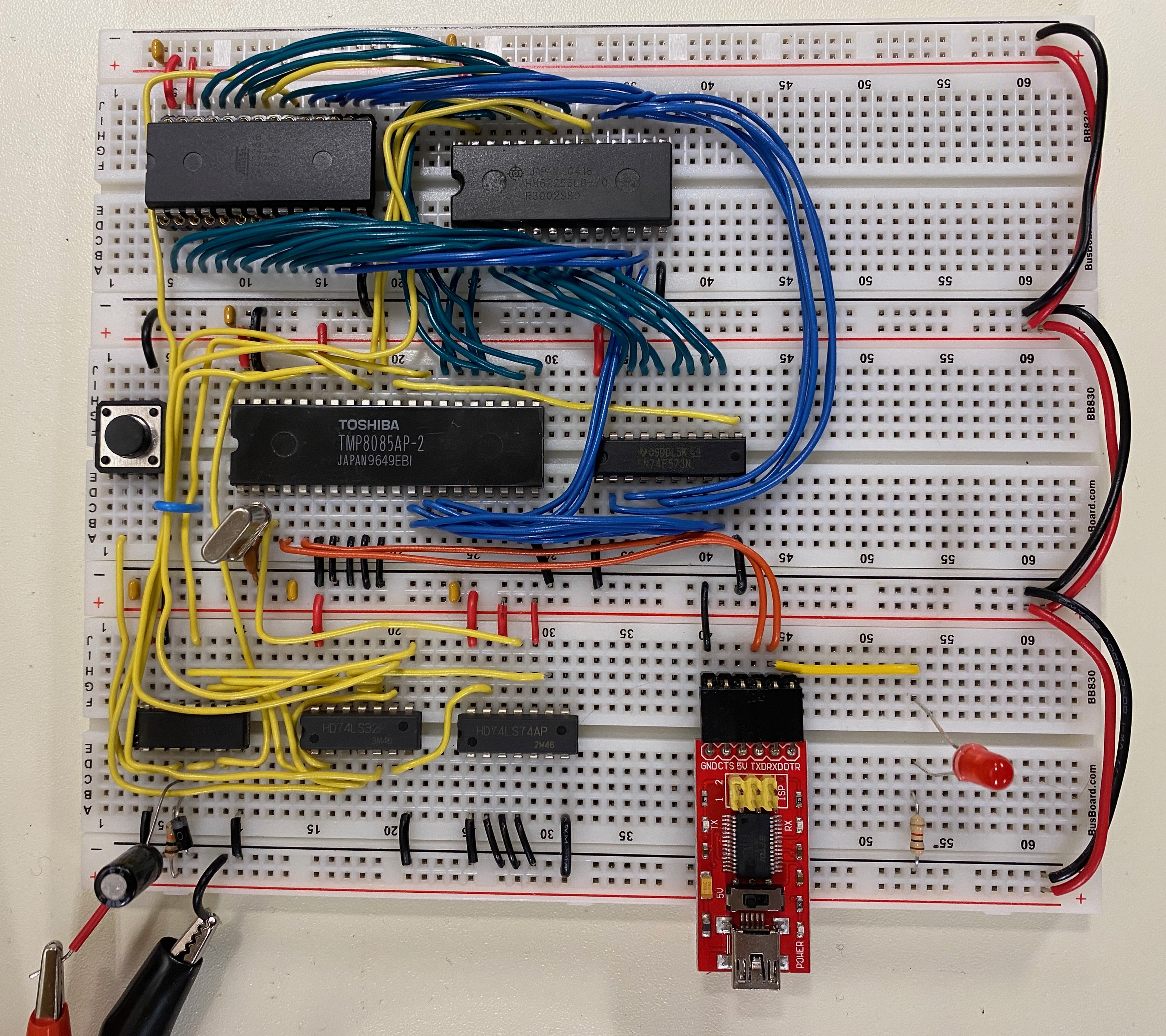
Step 5: Memory Addressing / Build Complete
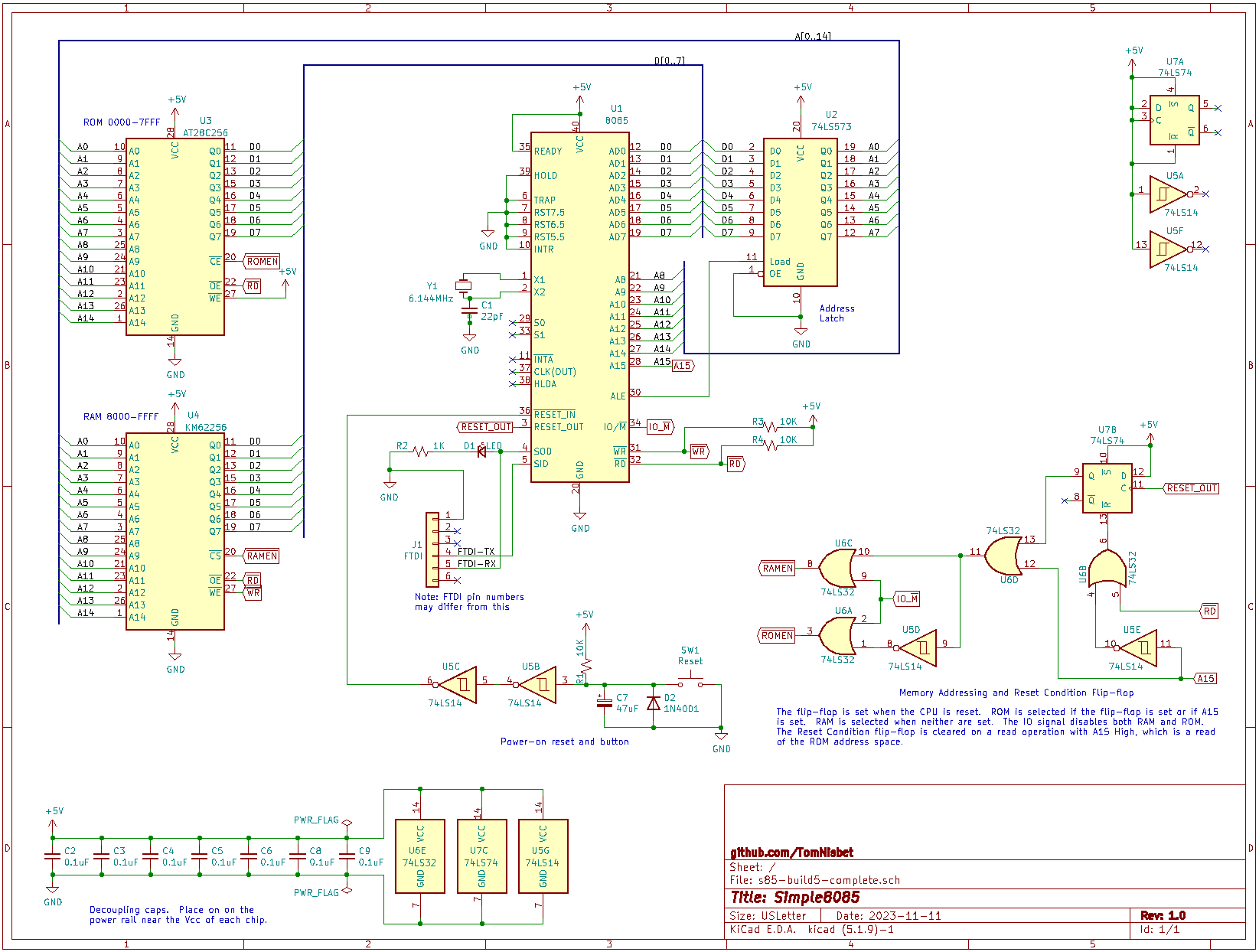
At this point, the processor, ROM, and RAM had all been proven, at least for simple operations. The address decoding and power-on jump logic were then added to swap the RAM and ROM starting addresses, making them compatible with the Explorer/85.
Rather than writing a new test, the entire Monitor ROM and Basic were loaded from the Explorer. Incredibly enough, it worked.