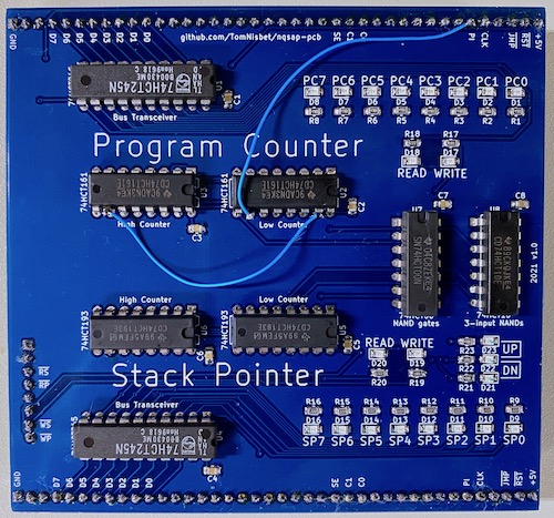
Program Counter and Stack Pointer
The Program Counter and Stack Pointer module implements two unrelated resisters. There are no interconnections or dependencies between the PC and SP, so they are co-located only because each design is simple and both could be implemented together on one board. The PC/SP board does not contain any register select hardware, so the read and write selects for the PC and SP are provided over the interconnects from the RAM/MAR board.
Program Counter
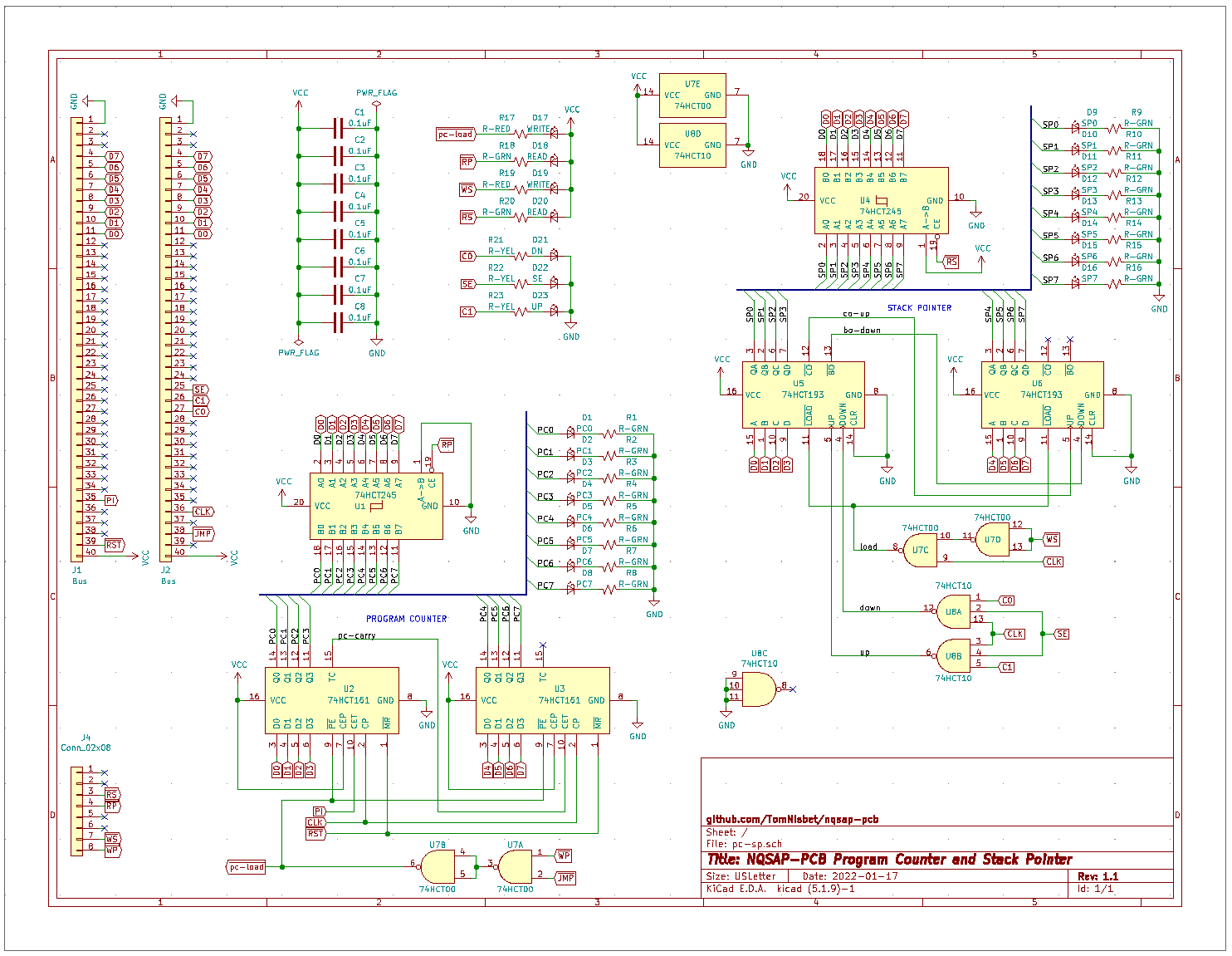
The Program Counter (PC) is implemented using two 74HCT161 4-bit counters. It increments on any clock cycle that has the Program Increment (PI) signal asserted. The PC is loaded with a new value when either the Write Program (WP) signal or the conditional JMP signal is low. The WP signal is produced by the register selects to perform an unconditional jump. The JMP signal is produced by the Flags Module.
Stack Pointer
The stack pointer (SP) is an 8-bit register with read/write access to the bus. It enables new instructions to push and pull registers (PHA, PLA) and to call and return from subroutines (JSR, RTS). There are also instructions to load the SP to and from the X register using the TXS and TSX instructions. If no stack operations are needed, the SP can also be used as a general-purpose register.
The SP is implemented using a pair of 74HCT193 4-bit up/down counters. Output to the bus is controlled via the usual 74LS245 bus transceiver.
The CLR signal is not used to reset the counter at system reset so the SP always starts in an unknown state. This isn’t a problem, because any programs that use the SP will want to initialize it to point to a free memory area before any stack operations are performed.
Unlike the 74HCT161, the 74HCT193 counters do not have a master clock or a count enable control. Counting is performed by pulsing the UP or DOWN pins and loading a new value is performed by pulsing the LOAD signal. Additional logic is used to AND these signals with the master system clock. To load a new value, the CLK and WS signals are combined.
Spare bus and microcode signals are in short supply. Rather than adding two new signals for the SP count up and down operations, a single Stack Enable (SE) signal was added. This is used in conjunction with the C0 and C1 carry control signals to control counting in the SP. The SE and C0 signals are asserted to count down and the SE and C1 signals are used to count up. These are combined with the CLK signal to produce the pulses for the DOWN and UP lines.
The shared use of the C0 and C1 signals means that the carry flag cannot be modified in the same microinstruction step where the SP is counting. The normal use of the C0 and C1 signals will not cause the SP to count because the SE signal will not be asserted. Note that the C0 and C1 signals will also be shared by the XY registers, so SP and indexing operations also cannot happen in a single microinstruction step.
Microcode
The SP counts up when pushing values to the stack and counts down when pulling values. There is no overflow protection, so the counter will quietly wrap if it hits the top or bottom of memory. The push operation uses a post-increment, so the value is stored and then the SP is bumped to point to the next available stack address. In other words, the SP always points to the address after the location of the value on the top of the stack. The pull operations pre-decrement, so the SP is moved to point to the value and then the value is retrieved.
Note that the Jump to Subroutine (JSR) uses a few tricks in the microcode. The value of the PC is needed to retrieve the subroutine address, but the PC also needs to be saved onto the stack before being overwritten with the new address. The ALU B register is used for temporary storage to save the subroutine address. The B register is not directly accessible by the user, so it is a good candidate for the microcode to use. The example below shows a JSR instruction at memory address 20.
| Address | Contents |
|---|---|
| 20 | JSR opcode |
| 21 | JSR address |
| 22 | next opcode |
After the instruction fetch, the PC will have the value 21 and JSR microcode performs the following steps:
- move the PC value to the MAR and increment the PC. MAR contains 21 and PC contains 22.
- read the subroutine address from RAM[21] and place it in B for temp storage
- move the SP value into the MAR and increment the SP.
- store the PC value (which points to the next instruction) in memory, i.e. push the JSR return address on the stack.
- move the B register value into the PC, effectively jumping to the subroutine
Note that the B register is needed because the PC value that is pushed to the stack is the one address after the location that hold the subroutine address. If the PC value was incremented and pushed before fetching the subroutine address, there would be no way to fetch the address because the PC has already moved past it.
An alternate approach that would not require temporary storage would be to push the PC while it was still pointing to the subroutine address instead of pointing to the next opcode. The RTS instruction would then need to increment the PC after fetching it from the stack. The downside to this is that the PC address on the stack would not be the true return address.
Bill of Materials
- 74HCT00 quad 2-input NAND gate(1)
- 74HCT10 triple 3-input NAND(1)
- 74LS161 4-bit counter (2)
- 74LS193 4-bit up/down counter (2)
- 74HCT245 8-bit bus transceiver (2)

